


Engineers from the University at Buffalo engineers have created technology that could lead to breakthroughs in solar energy, stealth technology and other areas - but they had to catch some rainbows first.
Qiaoqiang Gan, PhD, an assistant professor of electrical engineering at the University at Buffalo, and a team of graduate students developed a "hyperbolic metamaterial waveguide," which is essentially an advanced microchip made of alternate ultra-thin films of metal and semiconductors and/or insulators. The waveguide halts and ultimately absorbs each frequency of light, at slightly different places in a vertical direction to catch a "rainbow" of wavelengths.
"Electromagnetic absorbers have been studied for many years, especially for military radar systems," Gan said. "Right now, researchers are developing compact light absorbers based on optically thick semiconductors or carbon nanotubes. However, it is still challenging to realize the perfect absorber in ultra-thin films with tunable absorption band. We are developing ultra-thin films that will slow the light and therefore allow much more efficient absorption, which will address the long existing challenge."
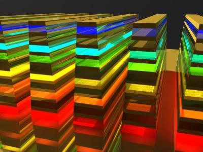
University at Buffalo engineers have created a more efficient way to catch rainbows, an advancement in photonics that could lead to technological breakthroughs in solar energy, stealth technology and other areas of research. Credit: University at Buffalo
Light is made of photons that, because they move extremely fast (i.e., at the speed of light), are difficult to tame. In their initial attempts to slow light, researchers relied upon cryogenic gases. But because cryogenic gases are very cold – roughly 240 degrees below zero Fahrenheit – they are difficult to work with outside a laboratory.
Gan helped pioneer a way to slow light without cryogenic gases. He and other researchers at Lehigh University made nano-scale-sized grooves in metallic surfaces at different depths, a process that altered the optical properties of the metal. While the grooves worked, they had limitations. For example, the energy of the incident light cannot be transferred onto the metal surface efficiently, which hampered its use for practical applications, Gan said.
The hyperbolic metamaterial waveguide solves that problem because it is a large area of patterned film that can collect the incident light efficiently. It is referred to as an artificial medium with subwavelength features whose frequency surface is hyperboloid, which allows it to capture a wide range of wavelengths in different frequencies including visible, near-infrared, mid-infrared, terahertz and microwaves.
In electronics there is a phenomenon known as crosstalk, in which a signal transmitted on one circuit or channel creates an undesired effect in another circuit or channel. The on-chip absorber could potentially prevent this. The on-chip absorber may also be applied to solar panels and other energy-harvesting devices. It could be especially useful in mid-infrared spectral regions as thermal absorber for devices that recycle heat after sundown, Gan said.
Technology such as the Stealth bomber involves materials that make planes, ships and other devices invisible to radar, infrared, sonar and other detection methods. Because the on-chip absorber has the potential to absorb different wavelengths at a multitude of frequencies, it could be useful as a stealth coating material.
Published in Scientific Reports


Comments