Characteristic for buried channel solar cells are that the front contacts (lighted surface) are placed in deep trenches, formed in silicon crystal. The idea, is to be minimized the width of the contact bars, by the increasing the contact thickness in deep. In this way the formed element has lower shadowing effect and additionally the contact resistance is decreased. The collected efficiency of the created by the light excess carriers is increased too.
Usually p-type Si wafers are used. By diffusion shallow n+ layer is formed on the front surface. By laser or mechanical grooving processes channels are cut. Deep trenches are formed, where the metal contacts have to be placed. The linear velocity of scanning of the places for the contacts bars is slow. After the cut out process the trenches are chemically etched, in order to remove the defects created by the grooving process. The next step is second diffusion for creation of emitter areas. Because of the complicated technological sequence, the production cost of these type elements is higher.
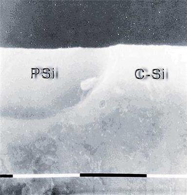
On the basis of patent was experimented new technology for realization of buried contact solar cells. Selectively formed thick porous silicon layer, created by standard anodization process was used. This layer easily could be removed by chemical etching.
This method has technological advantage compared with the used in the moment techniques – laser or mechanical grooving of the trenches.
In our experiments p-type Si wafers of 4–7 Ω.cm conductivity and 325 μm thickness were used to fabricate n+–p–p+ structure based solar cells. The diameter of the wafer was 50mm because of the size of the used Pt electrodes in the electrochemical tank. Porous silicon is a sponge-like fragile structure created in bulk silicon wherein pores are etched into the substrate by electrochemical etching using dilute hydrofluoric acid (10–20% HF concentration typically at 10–100 mA cm2 current density), which results in small silicon skeleton. Holes in silicon react at the surface with negative fluorine ions and dissolve silicon atoms from the substrate lattice. This property has been exploited to create PS selectively in the desired regions. If a p-silicon substrate has distinct n- and p-type regions that can be made easily by a diffusion process, PS will grow only on the p-regions whereas n-type regions will remain intact .
After the anodization step the porous silicon was removed from the surface of the wafer by the chemical etcher HNO3:H2O:HF, which has very good selectivity between PS and crystalline Si substrate .

Cross-section SEM picture of Si wafer after the anodization process
The technological procedure for formation of buried channels (trenches) is absolutely repeated and technologically cleared. The next phase was connected with the filling of the trenches with (Ag–Al) paste. Different technical methods were tested and it was chosen comparatively simple procedure.
I–V characteristics of two types of solar cells; one BCSC solar cells and the reference solar cells with conventional planner contacts (without buried contact, Al sputtered by photolithography) are shown below.

I–V Characteristics of reference and Buried Contact Solar Cells
As a result, the electrical parameters of BCSC are better compared with reference cell, due to the lower contact and sheet resistance in buried contacts compared with the classical planar metallization.


Comments